[Chinese Packaging Network News] As we all know, transistors are the most basic building blocks in electronic products. They are mainly used to generate circuits that can amplify, switch, regulate, and modulate signals. However, the manufacture of transistors is a highly complex process that requires high temperature, high vacuum equipment.
Today, engineers at the University of Pennsylvania have led a new method of manufacturing this device under the leadership of Prof. Cherie Kagan of the School’s College of Engineering and Applied Science: a liquid nanocrystal “ink†Forms sequentially deposit their components.
3D printing, nanocrystalline ink, 3D printed transistor technology, 3D sand insect net
Their latest research results have been published in the "Science" magazine. Some commentators believe that this technology opens the door to the incorporation of electrical components into flexible or wearable applications. In addition, this technology requires very low temperatures and is compatible with a wide variety of materials. Therefore, it can be expected that the scope of application will be quite broad.
Researchers based on nanocrystalline field-effect transistors are using spin coating techniques to draw flexible plastic backings. However, this process may eventually be accomplished through an additive manufacturing system, such as a 3D printer.
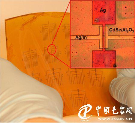
Researchers need to create nanocrystalline inks by initially dispersing nanocrystals, or spherical nanometer-sized particles, required for transistors in liquids. It is reported that Kagan's team has developed a total of four inks: a conductor (silver), an insulator (aluminum oxide), a semiconductor (cadmium selenide), and a combination of dopants. The conductor (a mixture of silver and indium). Scientists can control the device to transfer positive or negative charges by doping the semiconductor layer of the transistor with impurities.
“These materials are colloids, like the inks in inkjet printers.†Kagan said: “But you can get any attributes you want, such as conductors, semiconductors, or insulators, and our problem is how to place them on the surface. To form a functional transistor."
The electrical properties of these nanoinks have been confirmed separately, but they have never been combined before to form a complete device. "This is the first such study," said Choi, a member of the research team at the Advanced Institute for Geological and Mineral Research of Korea. "The results show that all the components of the transistor, including the metal layer, thermal insulation layer, insulation layer, The semiconductor layer, or even the doped semiconductor, can all be made of nanocrystals."
But to achieve them, they need to be layered or mixed in a fine pattern structure.
First, the silver nanocrystal particles were deposited by liquid on the surface of a flexible plastic using a photolithography mask and then rapidly rotated to draw it on a flat layer. The mask is then removed, leaving the silver ink in the shape of a transistor gate electrode. The researchers then spin-coated a layer of insulator ink based on alumina nanocrystals, followed by a layer of semiconductor based on cadmium selenide crystal particles, and finally coated with an indium/silver mixture with a mask. The source and drain of the transistor. Then at a relatively low temperature, the indium dopant diffuses from these electrodes into the semiconductor component.
"The point of using a solution-based material is that when you add a second layer, make sure that the first layer is not washed away," Kagan said. "We had to surface-treat nanocrystals, either when they were initially in solution or after deposition. This was mainly to ensure that they had the correct electrical properties and that they were able to stick together in the way we wanted."
Because the ink-based manufacturing process is done at a lower temperature (compared to the current vacuum-based approach), the researchers were able to make several transistors simultaneously on the same flexible plastic backing.
“Making transistors in larger areas and at lower temperatures has always been a goal pursued by many emerging technologies, such as the Internet of Things, large-area flexible electronics, and wearable devices.†Kagan said: “We have not yet completed all necessary developments. , so they can't print at the moment, but since these materials are based on the state of the solution, theoretically, they can be fully generated by additive manufacturing."
Pengpai Office Furniture Co., Ltd. , http://www.officefurniture-manufacturer.com